The Future of Fast & Affordable Infrared Sensors: Fully Printed PbS Nanocrystal Photodetectors
Why Printed Infrared Detectors Matter
Key benefits of this approach include:
Ultra-Low Cost: Material consumption is less than 0.3 mg per detector, costing below 20 cents per square centimeter
. High-Speed Manufacturing: The automated printing process takes only 14 seconds per detector
. Exceptional Sensitivity: These devices achieve a specific detectivity ($D^*$) of $\sim10^{12}$ cm $Hz^{1/2}/W$, putting them on par with state-of-the-art IR photodetectors
.
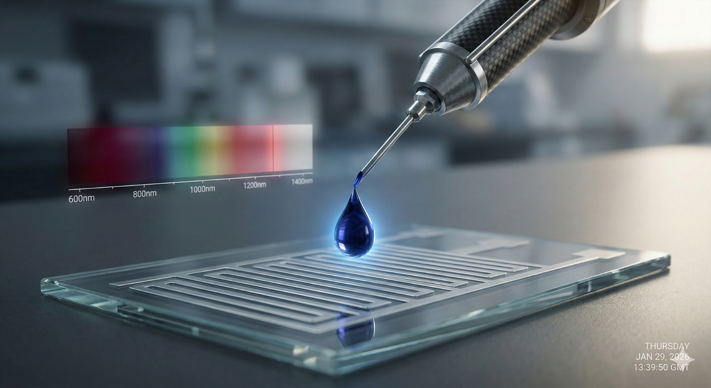
The Technology: Engineering the "Functional Ink"
The core innovation lies in the development of a specialized electronic ink. Standard PbS nanocrystals are typically capped with insulating oleic acid, which blocks electrical current
Replaced Ligands: They swapped oleic acid for perovskite-like methylammonium iodobismuthate ligands, which facilitate efficient charge transport
. Optimized Solvents: A ternary solvent mixture (DMF/NMF/DMSO) was used to ensure smooth film formation and prevent cracking during drying
. Added Polymers: By adding poly(vinylpyrrolidone) (PVP), the team improved the ink’s stability and eliminated the "fractal crack patterns" that usually ruin printed films
.
Two Paths to a Fully Printed Device
The researchers explored two different printing architectures:
| Feature | Approach (i): All-Inkjet | Approach (ii): Robot & 3D Printing |
| Method | Layer-by-layer inkjet printing.
| 3D-printed ABS frame + robotic droplet dispenser.
|
| Speed | Relatively slow (3 mins per detector).
|
Extremely fast (14 seconds per detector).
|
| Performance | Functional, but prone to nozzle clogging.
|
Superior stability, high detectivity, and scalable.
|
What’s Next?
While these specific sensors are designed for infrared detection, the "PVP-modified ink" strategy is expected to work for a wide range of materials. This paves the way for the low-cost production of solar cells, thin-film transistors, and wearable health monitors.
- Source: YousefiAmin, A., et al. (2019). Fully Printed Infrared Photodetectors from PbS Nanocrystals with Perovskite Ligands. ACS Nano, 13(2), 2389-2397. [DOI: 10.1021/acsnano.8b09223]